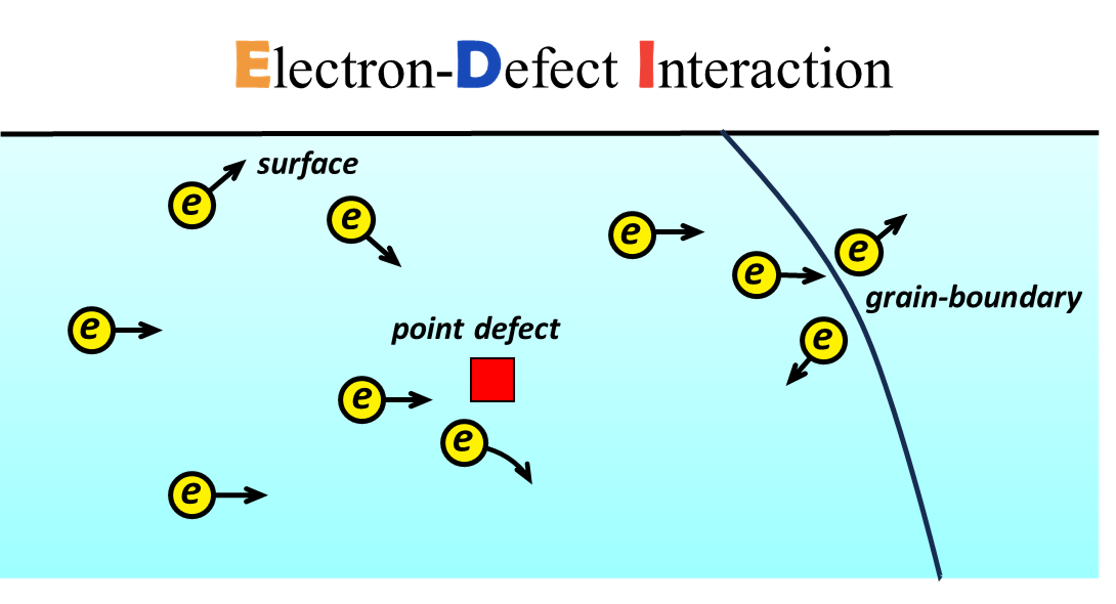
Electron-defect interaction is crucial to many processes and applications such as charge transport and light absoprtion/emssion. EDI (electron-defect interaction) is a software package to calculate the electron-defect interaction and the associated properties from first principles.
Capabilities
Currently, EDI can calculate the following quantities for charge-neutral point defect:
- EDI matrix
- scattering rate/relaxation time
- carrier mobility/conductivity
We are also implementing or will implement methods for calculating:
- charged defects
- surfaces
- grain boundaries
Example
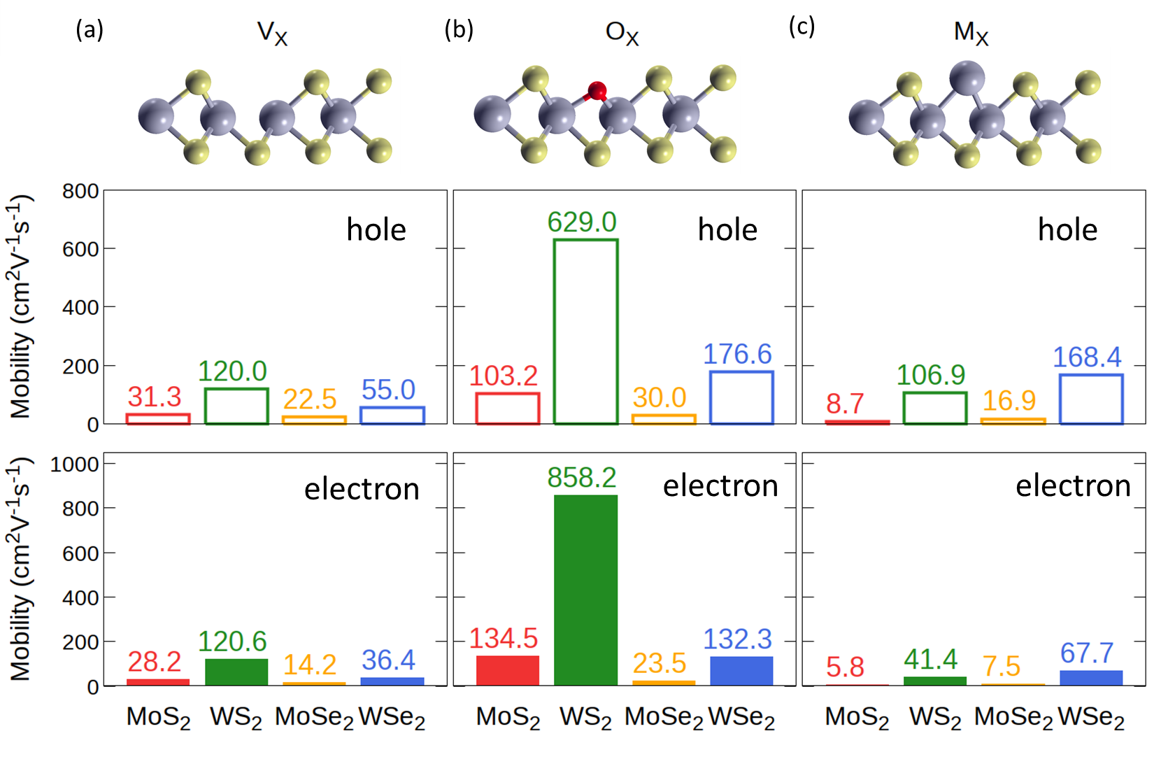
Here is the point-defect-limited mobility in monolayer transition metal dichalcogenides calculated with EDI. The defect concentration is $10^{12} cm^{-2}$.

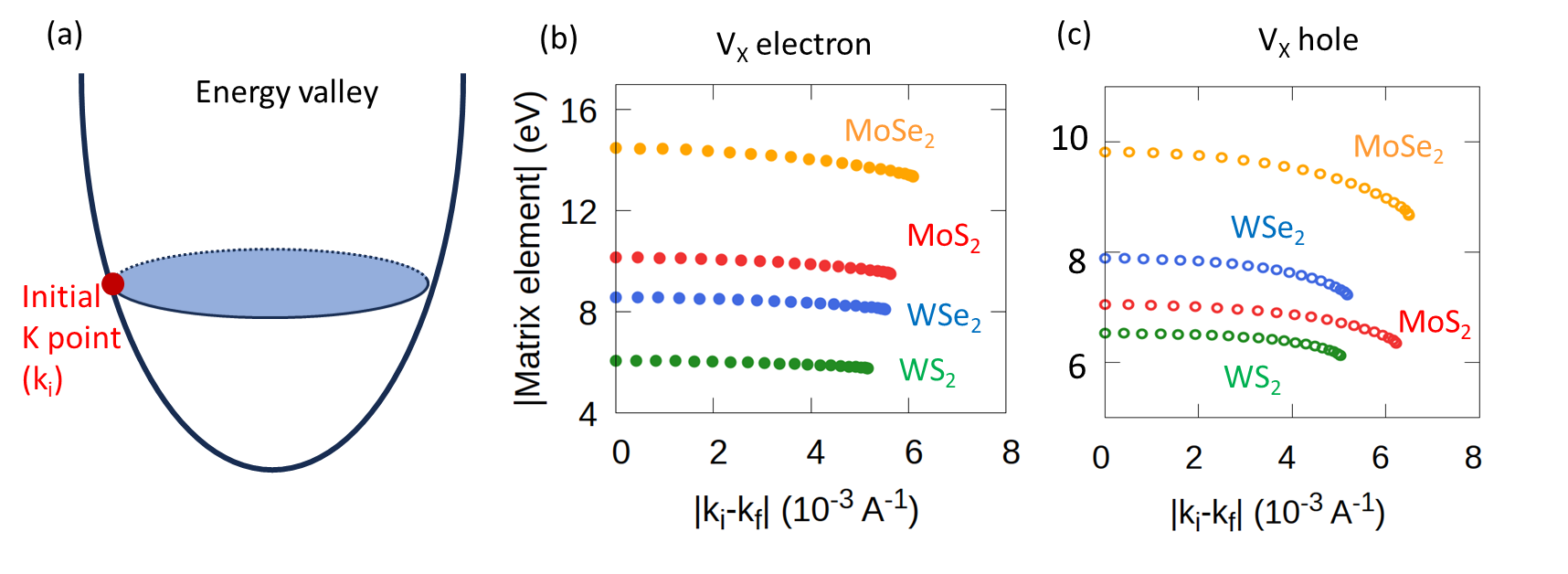
Below are matrix elements of EDI for chalcogen vacancy.

For details of the above figures, see the publication.
Reference
Zhongcan Xiao, Rongjing Guo, Chenmu Zhang, and Yuanyue Liu. Point Defect Limited Carrier Mobility in 2D Transition Metal Dichalcogenides. ACS Nano. DOI: 10.1021/acsnano.4c01033